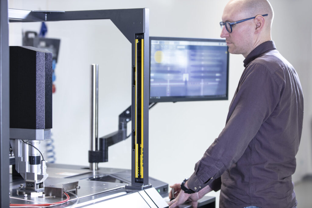
The technically sophisticated probe system TS2000-HP from MPI Advanced Semiconductor Test offers SwissSEM a wide range of testing options for power semiconductors for renewable energies and e-mobility solutions.
Technical systems that are required to convert primary energy into electrical energy have already undergone numerous paradigm shifts. The focus now lies primarily on efficient and sustainable energy supply and use, with components such as power semiconductors playing a key role.
The company SwissSEM Technologies AG has specialized in the development and design of these specific components. The experts are particularly concerned with voltage classes such as those used in the rapidly expanding automotive and renewable energy market segments. A dedicated R&D team develops the characteristic power semiconductor chips and packages and tests them in a specially designed test laboratory. Hilpert electronics supports the design experts as a provider of products and services for quality assurance in electronics production with tailor-made production technology.
“Especially in the development phase, the rapid and efficient testing of the design properties of power electronic packages in accordance with strict quality specifications is of crucial importance,” explains Roger Stark, Head of Test Laboratory SwissSEM CH. For this purpose, SwissSEM relies on the semi-automatic high power probe system TS2000-HP from MPI Advanced Semiconductor Test, which is delivered turnkey by Hilpert electronics. The shielded probe system is designed for measurements up to 10 kV 600 A and offers a wide range of functional advantages and configuration options. At the same time, the SwissSEM developers benefit from both the close collaboration with Hilpert electronics and the direct contact with the prober manufacturer MPI and its extensive services.
Precise measurements – intuitive operation
The high-precision TS2000-HP can be used during prototype development to check whether a design meets the process requirements. The system is characterised by a wide range of functional features. For example, a well-thought-out user interface that guides the user through the steps to be carried out and thus minimizes incorrect operation. In addition, the operator can familiarize himself with the machine within a very short time through “learning by doing”. “I was able to convince myself of the diverse product features of the MPI-Probers during previous employment relationships. For this reason, and because the system fits well into the requirements and cost framework, SwissSEM also chose the TS2000-HP,” says Stark.
Flexible design-specific wafer testing
The power semiconductors to be tested are characterized by very fine structures and thus by a specific construction. Nevertheless, the MPI system is able to contact the components precisely. “The TS2000-HP impresses not only with its fast and efficient measurements at the on-waver level. Rather, the MPI prober navigates from chip to chip across the entire wafer for the functionality test as part of the semi-automatic work process. The number of wafers to be tested can vary depending on the design. Furthermore, process and production corrections are possible in different phases,” explains Stark and at the same time refers to the extremely efficient and functional software. The user-friendly program allows corrective action to be taken at any time and can also be updated independently by the user.
Another distinctive feature is the ability to place an additional camera on the side, thus providing an additional viewing angle in addition to the bird’s eye view through the camera attached to the top of the microscope. “This additional horizontal perspective has proven to be particularly advantageous when making contact with multiple needles,” emphasizes Stark.
MPI continuously develops the functionalities of its probe systems based on customer requirements, among other things. The manufacturer has designed a special interface panel for SwissSEM. As a further example, a specific Chuck-Liquid-Tray with a Teflon frame can be cited. “This special tray allows chips to be contacted directly even if they are installed in a housing. This makes design testing much easier. The Prober system from MPI fully meets our requirements,” says Stark happily.
If customer-specific system adjustments are relevant in practice, other companies also benefit from the innovations.
“Factors such as personal exchange, timely answers to specific inquiries, flexible and outstanding support as well as a wide range of optimally adapted services characterize the collaboration. With Hilpert electronics and MPI Advanced Semiconductor Test, we have reliable partners at our side who actively support us in innovative developments,” concludes Stark.


